
On 3 June 2026, the Dutch firm ASML Holding N.V. became Europe’s most valuable publicly listed company ever with a record market capitalisation of nearly $ 668 billion. By doing so, it crossed the earlier record of $ 650 billion set by Novo Nordisk in June 2024. ASML is the world’s only maker of extreme ultraviolet (EUV) lithography tools and the primary producer at scale of deep ultraviolet (DUV) lithography tools that are used for making advanced chips. Its market valuation has massively increased in recent years due to the surge in demand for cutting-edge chips for AI infrastructure and the resultant enhanced investment in semiconductor fab facilities by many chipmakers all over the world.

Nevertheless, a month later, on 27 July 2026, ASML’s stock dropped more than 5.8% and continued to drop for the next two days, wiping off billions from its market value. The reason: reports from China that an unnamed Chinese company was close to challenging ASML’s near monopoly in mass manufacturing of immersion DUV lithography machines. It is estimated that the company’s stock finished the month of July down at least 18%.
ASML’s stock had risen almost 86% in the first half of 2026 with a 24% surge in June itself thanks to positive endorsements by Elon Musk and others. On 7 June, Elon Musk on X called ASML ‘arguably the greatest company in Europe’ and which needed to be ‘treasured and supported.’ Musk also made a virtual appearance at the ASML’s technology conference on 11 June where he spoke in a fire-side chat with the ASML’s CEO Christophe Fouquet. This chat had been preceded by Musk’s announcement in March 2026 of a joint venture between SpaceX and Tesla named Terafab that would manufacture chips for both the companies in Texas, USA. The project will have ASML as a key supplier of equipment and its total investment across multiple phases is estimated to reach almost $ 119 billion. For comparison, the Terafab building in Texas is expected to have more than ten times the floor space of TSMC’s largest existing fabs.
About ASML
ASML (originally Advanced Semiconductor Materials Lithography but later legally shortened to ASML) was founded in 1984 and is headquartered in Veldhoven, the Netherlands. It was jointly created by Philips and Advanced Semiconductor Materials International (ASM) to develop lithographic systems for chipmakers.
In 1986, it launched its first commercial system, the PAS 2000 stepper, and also began its most valuable and on-going partnership with the lens manufacturer Carl Zeiss. By 1995, ASML had become a fully independent company, listed on the Amsterdam and New York stock exchanges.
In the early 1990s, ASML began producing dry DUV systems that are still being used by chipmakers all over the world. In 2001, it introduced its TWINSCAN system that uses dual-stage technology to expose one wafer while simultaneously measuring and aligning the next wafer.
In 2003, it was ready with its first immersion DUV system that could print much smaller features on the wafer by projecting light through a thin layer of ultra-pure water between the wafer and the lens. This layer itself acts as a lens to enable exposure at 38 nm or less, allowing for further miniaturisation of semiconductors. In 2006, ASML began shipping the first volume production machines based on this technology (XT:1700i), followed by TWINSCAN XT:1900i scanners the next year. Along with these innovations, in 2007 it also adopted the strategy of ‘Holistic Lithography’ that sought to optimise the chip manufacturing process before and after the lithography process as well.
In 1998, ASML formed an R&D industrial consortium named EUCLIDES (Extreme UV Concept Lithography Development System) with Zeiss, synchrotron light source supplier Oxford Instruments, and other suppliers to develop EUV technology. By 2006, the first EUV prototypes were ready and were shipped to IMEC (Belgium) and SUNY (Albany, New York) for further research to fit it into the chip-making process. In 2008, SUNY achieved the critical breakthrough and the following year, ASML began work on its production at Veldhoven. The first pre-production EUV prototype was ready in 2010, but it needed many more years of collaborative R&D with its key customers such as Intel, Samsung and TSMC before these EUV lithography tools became ready for commercial use.
To accelerate this process, ASML also acquired in 2013 for $2.66 billion the US company Cymer that specialises in manufacturing sophisticated light sources. In all, ASML claims to have spent € 6 billion over 17 years to develop the EUV technology that has now made it Europe’s most valuable corporate asset.
It was only in 2019 that the first commercial products powered by chips produced using ASML’s EUV machines were launched. These were Samsung’s Galaxy Note10 and Galaxy Note10+ smartphones. By the end of 2021, there were 127 such EUV machines being used by chipmakers all over the world.
To compare, DUV lithography uses light with wavelengths between 193 nm and 365 nm whereas EUV lithography uses an extreme short wavelength of 13.5 nm that enables direct single patterning for minute features on advanced nodes. For comparison, the distance between two neighbouring silicon atoms is 0.235 nm.
By 2024, ASML was ready with the even more advanced high numerical aperture extreme ultraviolet (High NA EUV) lithography system. This scanner enables even more precise patterning (sub-2nm) and is currently being used by Intel Foundry on Intel 18A process node to produce its latest processors.
ASML and global market share
The global market for EUV lithography is valued at around $14 billion and is expected to go up to $58 billion by 2035. An EUV system costs anything from $200 million to $ 400 million per unit for High NA EUV scanner. ASML has no competitor in this sector. In December 2025, Reuters reported that some researchers in Shenzhen, China, had secretly built an indigenous EUV prototype but, even if true, it will be many years before a Chinese company is able to produce a commercially viable EUV lithography scanner and challenge ASML’s monopoly.
The DUV lithography global market was estimated at $10.6 billion in 2025 and is expected to grow 5.6% per year in the next decade. Depending on features and maintenance contracts, the cost of an immersion DUV system ranges from $40 million to $70 million per unit while dry DUV systems range from $25 million to $45 million per unit. In immersion DUV technology, ASML’s only competitor is Nikon Corporation and, in dry DUV systems, both compete with Canon Inc and the Chinese company Shanghai Micro Electronics Equipment Co., Ltd. (SMEE).

ASML, Nikon and Canon together account for approximately 85% of the global market with ASML taking the lion’s share (almost 55%) due to its established collaboration with top foundries like Samsung, Intel, and TSMC and its proven ability to vertically integrate into next generation technologies. The difference in technology and scale between ASML and Nikon shows in the gap between their market capitalisation which, as of August 2026, was around $680 billion for ASML and only $4 billion for Nikon.
In recent years, as demand for chips has grown due to increased digitalisation and AI boom, demand for ASML’s older dry DUV equipment has also surged. The simpler chips that they help produce are needed for most gadgets and even many layers on most advanced chips are printed on these machines. For this reason, ASML has been buying back its older machines to resell them after refurbishing and has also been working on the next generation dry DUV technology.
China’s biggest hope to challenge ASML’s lithography dominance is the state-backed SMEE. However, as per its website, the most advanced machines it produces at present, SSX600 Series, are designed for both critical and non-critical layers at 90 nm, 110 nm and 280 nm nodes and enable mass manufacture of 200mm and 300mm wafers. In 2023, some Chinese media reports suggested that it had begun shipping its next level immersion DUV system capable of producing chips at 28 nm node (SSA800 Series) to some Chinese fabs but these reports were never verified. In 2026, another Chinese company, Shanghai Aishengna Electronic Group, most likely an affiliate or spin-off of SMEE formed in 2023, was named as the manufacturer of China’s first immersion DUV lithography scanner. Technology-wise, however, many experts believe that this scanner is not even up to ASML’s NXT:1980i series that was first launched in 2015.
ASML in US-China rivalry
In 2018, the Dutch government gave a license to ASML to export its most advanced EUV machine to a Chinese customer, identified by some reports as China’s biggest chipmaker Semiconductor Manufacturing International Corporation (SMIC). A high-level campaign by the US to pressurise the Dutch government ensured that the shipment never reached China. Reportedly, a classified intelligence report was shared with the Dutch prime minister on his US visit to convince him.
While EUV technology was blocked, ASML continued to sell its DUV lithography machines to China. On 1 September 2023, under more US pressure, the Dutch government extended export controls to the most advanced DUV machines (TWINSCAN NXT:2000i and subsequent systems). These were further expanded to cover even older DUV immersion lithography systems (TWINSCAN NXT:1970i and TWINSCAN NXT:1980i) w.e.f 7 September 2024. Also, more Chinese fab facilities were added to the US list of restrictions.

In April 2026, some US lawmakers introduced a bill titled “Multilateral Alignment of Technology Controls on Hardware Act” (MATCH Act) to specifically restrict export of semiconductor manufacturing equipment and related components to ‘covered entities’ in ‘adversary countries’ to protect the US and its allies’ advantage in this ‘foundational technology.’ It seeks controls not only on the US-origin chips manufacturing equipment but also on every country that produces covered tools and is not a country of concern. The tools covered in this bill include all DUV immersion photolithography machines ‘through silicon via deposition and etch tools, cryogenic etch equipment, and cobalt deposition equipment, regardless of overlay or other performance characteristics.’ Moreover, the bill also subjects the servicing of these machines in covered facilities to licensing requirements. Crucially, most Chinese fabs still rely on ASML’s TWINSCAN NXT:1980i series scanners and, if MATCH Act is enacted, these would no longer be serviced or upgraded by ASML, severely crippling semiconductor manufacturing in China.
Even without EUV lithography technology, chipmakers can use multi-patterning techniques to produce more advanced chips (down to 7 nm node) with immersion DUV lithography machines although the process is slow and yields are lower. In multi-patterning, the wafer is run through the DUV lithography scanner multiple times to build a single layer and requires machines with high DCO (dedicated check overlay) accuracy. Every generation of ASML’s immersion DUV machines has better DCO than its predecessor. SMIC reportedly uses NXT:1980i machines to produce 7 nm microchips for Huawei Technologies and this is what the MATCH Act targets as it tries to limit Chinese manufacturing only to mature nodes of 28 nm and above. This has spurred China to develop its own advanced lithography tools but, given the highly complex and advanced technology, materials, and ecosystem needed, it is not so easy to achieve. According to an expert, the Chinese technology at present in this area is at the level in which ASML was in 2004.
The ‘extraterritorial’ and sweeping nature of the bill’s scope as well as its potential effect on ASML’s revenues have raised concerns in the Netherlands too.
Despite export restrictions, almost one-third (33%) of ASML’s total revenue in 2025 came from its exports to China. Things, however, changed in 2026. In contrast to 2025 figures, revenue from China slid to 19% of total revenue in the first quarter of 2026 and declined further to 14% in the second quarter. Nevertheless, the company in July 2026 claimed that, thanks to its non-Chinese customers’ capacity enhancement plans due to the AI boom, its order intake remained strong. It unveiled plans to add 30% to its DUV immersion capacity of around 130 for 2027 and a similar percentage increase to its EUV capacity of around 65 for the next year.
At the same time, if servicing and technical support contracts for already installed machines in China are also banned, ASML stands to lose not an insignificant amount of recurring and predictable revenue. Some of it can be offset by new customers such as India’s Tata Electronics with which it signed a deal in May 2026. With a total planned investment of $11 billion, the Tata fab in Dholera (Gujarat) is India’s first 300 mm (diameter of silicon wafers) commercial semiconductor fab. Tata has also signed MOUs with many other key companies across the entire semiconductor ecosystem such as Tokyo Electron, Merck Electronics, ROHM, Intel, and Powerchip Semiconductor Manufacturing Corporation (PSMC, Taiwan). Unlike geopolitical tensions with China, India and the EU have already in place a partnership since 2023 in the form of EU-India Trade and Technology Council (TTC). This TTC has a strong focus on semiconductors and has laid particular emphasis on increasing cooperation in facilitating investments as well as joint R&D in this sector.
The future of ASML’s monopoly and EU’s open strategic autonomy
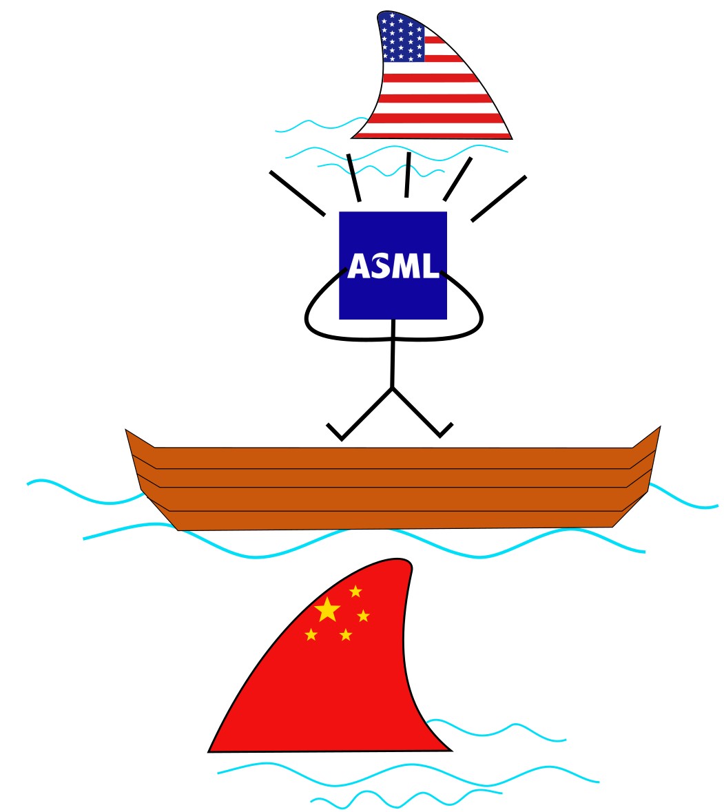
Although it would take some years for Chinese companies to catch-up with ASML’s technology, China’s decisive steps towards self-sufficiency in DUV immersion lithography have shown the ineffectiveness of US and European export bans as a long-term solution. These bans may have constrained China in the AI race for the time being, but these have also pushed ASML’s biggest customer into becoming its biggest future competitor. At the same time, it has eroded the geopolitical leverage and bargaining power that ASML’s monopoly gives EU.
The EU itself had enacted its Chips Act in 2023 to pursue self-sufficiency across the chips value chain, framing it as imperative for its strategic autonomy and technological sovereignty. More recently, recognising Europe’s structural weaknesses in this sector, some experts have been advocating ‘open strategic autonomy’ defined as a strategy of ‘Allied Autonomy, European Indispensability.’ In other words, instead of complete self-sufficiency across the semiconductor ecosystem, EU needs to leverage its grip over the critical chokepoint (lithography tools) in chips value chain to embed itself in strategic partnerships with key players, thus making its indispensability a guarantee against supply chain disruptions. China’s mass production of lithography tools will unsettle European indispensability in the semiconductor value chain and seriously undermine this framework of open strategic autonomy.
For more about lithography: Lithography AKA Rock Drawing
Related content by author
-
The Curious Case of Nexperia: Strategic Technologies and Strategic Challenges
-
European Union’s Chips Diplomacy: CHIPDIPLO and Other Diplomatic Initiatives concerning Semiconductors
-
European Chips Act 2023: What is it? And Why has EU proposed a new European Chips Act 2.0?
-
What is Strategic Autonomy? And why can’t Europeans stop talking about it?
-
Semiconductors and the European Quest for ‘Technological Sovereignty’: What is it exactly?
-
CHIPS for Chips: From Global Interdependence to National Self-Sufficiency?
Frequently Asked Questions (FAQ)
Ques: What is ASML?
ASML is a Dutch company that makes highly advanced photolithography machines used to manufacture semiconductor chips. Its machines project patterns onto silicon wafers to create tiny structures such as transistors. ASML is the world’s only manufacturer of EUV lithography systems and is also a major supplier of DUV systems.
Ques: What is DUV lithography?
Deep Ultraviolet (DUV) lithography uses ultraviolet light, mainly at wavelengths such as 248 nm and 193 nm, to transfer circuit patterns onto a silicon wafer. DUV is used to manufacture a wide range of chips, from mature-node devices to advanced chips, with 193 nm immersion DUV capable of producing very small features through multiple-patterning techniques.
Ques: What is EUV lithography?
Extreme Ultraviolet (EUV) lithography uses extremely short-wavelength light at approximately 13.5 nm to print very small patterns onto silicon wafers. The shorter wavelength allows manufacturers to create smaller features with fewer patterning steps, making EUV particularly important for advanced semiconductor nodes such as 7 nm, 5 nm, 3 nm and 2 nm-class processes.
Ques: How is DUV lithography different from EUV?
The main difference is the wavelength of light used. DUV uses wavelengths such as 193 nm, while EUV uses 13.5 nm. Because EUV has a much shorter wavelength, it can print smaller features more efficiently and reduce the number of patterning steps required. However, EUV systems are far more complex and expensive, while DUV remains essential for both advanced and mature semiconductor manufacturing.
Ques: What is immersion lithography?
Immersion lithography is a technique in which a thin layer of liquid, usually ultrapure water, is placed between the final lens and the semiconductor wafer during exposure. The liquid increases the effective numerical aperture of the optical system, allowing smaller features to be printed. 193 nm immersion DUV (193i) is one of the most important lithography technologies used in modern semiconductor manufacturing.
Leave a Reply