
Here begins the beginner’s guide to lithography.
Yes, that is what the name means if you separate ‘litho’ and ‘graphy’. Doesn’t seem that scary now does it? The name is very literal to the process conducted. The rock in question is our silicon wafer and we create patterns on it for further processing. It is a very crucial process as it directly determines the transistor density which is directly proportional to the amount of data it can process at a time. Patterns are either printed or written on the wafer. Let us go through the process step by step.
Basics of optical lithography

First, we coat the wafer in a liquid state compound called photoresist. As the name suggests, this compound changes its properties when light is shined on it. The wafer is then spun around for a determined time and rotations per minute to ensure uniform coating. The same way we use our handheld utensil (I don’t know what you use) to evenly coat bread with butter or jam so that we get every flavored bite, same principle is used here. The compound is subsequently hardened by heating either in an oven or on a hot plate. This concludes the application of material on which the pattern will be printed.

We move on to exposure of the photoresist to our energy source which will be light here. A mask is put on top first. A mask has the design which will be printed on the wafer. It is fed into the machine and it adjusts the position accordingly. The light source determines the minimum feature size. The two common exposure systems are step-and-repeat (stepper) and step-and-scan (scanner). Stepper exposes the entire chip onto its designated area once and then moves on to the next area and repeats the exposure. An exposed area is not revisited again. Scanner works a bit differently, light is passed through a thin slit and it scans the mask slowly onto the wafer for one area. After the scan is done it moves onto the next. Stepper is one camera flash onto an area and scanner is like me ironing my shirt onto the area. Scanner is better for high resolution lithography.

Lenses are used to focus light through the mask onto the wafer. Magnification depends on end-user requirement. Masks are made of materials that block/absorb light where not required. This is a very important process that occurs now, during exposure the photoresist changes properties as I had pointed out earlier. There are two ways it can go. It either hardens (insoluble) or softens (soluble) in response to light. Positive photoresist softens and negative photoresist hardens.
After exposure is complete the wafer is developed. In the good old days of analog technology, camera film reels had to be developed inside a solution called developer. This occurred in rooms with little to no external light with only a small red light for vision due to it having the highest wavelength, leading it to have the lowest energy which prevents any changes in the image due to unneeded excitation. The same principle is used here. The developer dissolves the soluble part of photoresist. The wafer is either immersed in developer or developer is dispensed on it while it spins. The latter is better for high resolution. The developer is dried off and then sent for further processing.

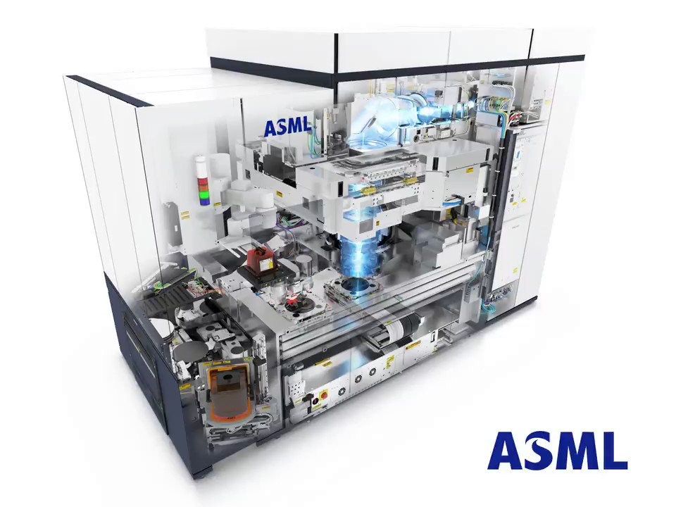
This was the basic run-down of optical lithography. After the process following development is completed, like etching, doping, or deposition, the photoresist is cleaned off using wet chemicals or etched out using oxygen plasma called ashing. It seems like a simple enough process when done on a micrometer scale, the problems all start when we go down into atomic level. Suddenly all sorts of problems crop up- problems of such magnitude that only one company in the world has managed to solve a size-able chunk of them, ASML.
The problems begin…
The first problem is your light source. For a smaller feature size, we need smaller wavelength. The spectrums used commonly are Mid-Ultraviolet (MUV: 300-400 nm), Deep-UV (DUV: 100-300 nm), and Extreme-UV (EUV: 10-121 nm). MUV uses i-line mercury lamps and gives features of 350-500 nm. DUV uses Krypton Fluoride (KrF: 248 nm) or Argon Fluoride (ArF: 193 nm) and gives a feature size of 38-250 nm. EUV uses a completely different mode of light generation; it uses Tin (Sn) plasma (ionized gas) to emit light with a wavelength of 13.5 nm and gives a feature size of 2-7 nm.
I must have bored you, dear reader, with the overwhelming number of figures that I just threw at you so let me put a scenario in front you; you go for a surgery and just after the anaesthetic starts to kick in, you see your surgeon walk in with a sword, place it on the surgery tray and helplessly watch him throw the scalpel in the bin. That is the same scale we are operating in when dealing with such light sources. EUV already has a problem in generation, not being content with just that, when light wavelength reaches atomic level scale, lenses are useless. You cannot focus it by optical lenses. Zeiss manufactures lenses for MUV and DUV sources, yet they have their hands bound in this case. EUV utilizes precision mirrors for focusing light.

(Reference: Left: Ansys Right: SemiSlides on YouTube)
This was just the first problem which also brought with it a bonus issue. Now, we go towards exposure conundrums like: a) specialized photoresist which only reacts under a high enough energy; b) masks which need to reflect instead of absorbing light, c) high aspect ratio: the resist thickness is the same with feature width getting smaller, this causes the photoresist to weaken and it becomes prone to deformations; d) standing waves caused by interference in incoming and reflected light, it causes ripple like sidewalls reducing process area; e) low depth of field where a tiny variation causes loss of focus; f) overlay accuracy needs to be high, if a feature is not overlaid properly the device becomes useless. Many more problems exist outside of the ones listed here. If I keep listing it out you will get bored and leave, and I will get sad, so let me give you the second half of this proverbial lithography coin.
The alternative: electron beam lithography
I have been using the word print for so long you must have internalized it and accepted it as the only way. So how about a technique that is free from all optical problems and it does not even need a mask. Yes, dear reader, I am talking about writing. Electron beam lithography does exactly that. Stepper motors control the position of the wafer while the electron beam draws the pattern on the electron beam resist (name change due to difference in excitation source). It has some problems of its own like electron scattering and electron dose control, dose being the number of electrons on the area per unit time. Yet all of these problems pale in comparison to one big problem.

I want to ask you, when was the last time you got your portrait done in a professional studio? Was it done by camera or did the person there draw you, or paint you? If you were going for a painting, you would have to sit there for the whole day in a single pose, while on the other hand a photograph is a one and done. Maybe some extra for fine tuning of your photo, my point being it is a very fast process compared to painstakingly painting your face. Electron beam lithography is very slow compared to optical lithography. By industrial standards, it is criminally slow. What may take optical one second to do, it takes electron beam around 1,000-10,0000 seconds. For this reason it is the preferred method in research due to the lack of mask manufacturing.
The nature of this method, being what it is, requires the highest level of clean room classification and special lighting to prevent resist triggering outside of controlled exposure. Special yellow lighting or safe lighting are used with wavelengths above 500 nm inside the room. They also filter out UV and blue wavelengths that may be emitted.
The idea of this method is quite simple, even primitive considering how long we have been drawing on rocks. Practical application is always the biggest obstacle that engineers and scientists have to face. This is a trend you will notice in every single method used in semiconductor manufacturing. The theory behind it is disgustingly simple, and yet there is a reason why it is such a highly specialized industry with such a high barrier for entry.
Frequently Asked Questions (FAQ)
Ques: Why is lithography so important?
Lithography controls the process area. Without a very high resolution lithography system, transistors would not be as small as they are today. It is the same as trying to print a 4K image with a printer from 2010, you will get a blurry mess of a picture.
Ques: Why do photoresists change with light source?
Different light sources have different energies. The lower the wavelength, higher the energy. A photoresist is manufactured to harden or soften at a specific energy. Using a light source with energy lower than the required energy will cause inadequate opening of process area. The same goes for higher energy as unwanted reflection may cause more than the required area to be affected.
Ques: Why are mirrors required for EUV lithography?
EUV light has very high energy, it gets absorbed by glass. Only specially designed mirrors are used called multilayer Bragg mirrors. These have alternating thin layers of silicon and molybednum repeated around 40-50 times. These mirrors have a reflectivity of around 70%. The rest is absorbed, refracted or transmitted.


Leave a Reply