
HEMT devices require a special type of chemical vapour deposition technique, one that can handle a high amount of throughput for industrial standards. The other process used for III-V compound semiconductors is called molecular beam epitaxy (MBE), this techniques gives better uniformity and controllability during fabrication, but is very slow.
Introduction to MOCVD
MOCVD is also called organometallic chemical vapour deposition (OMCVD), metal organic vapor phase epitaxy (MOVPE), and organometallic vapour phase epitaxy (OMVPE). It is the process of growing compound semiconductor layers on a wafer using pyrolysis reactions between the vapours of a volatile organometallic compound and a gaseous hydride.
A pyrolysis reaction is the degradation of compounds in the absence of oxygen at high temperatures ranging from 500℃ to 1200℃. On the heated substrate, the precursors decompose and react to form a thin film or epitaxial layer of the desired material. Epitaxy is the technique used to grow a thin crystalline film (epitaxial layer) on a crystalline substrate, where the deposited layer adopts the crystal structure and orientation of the substrate.
Reacions in MOCVD
The simplest case of pyrolysis decomposition for epitaxial growth is:
where is R an organic radical of some unspecified form but generally of lower order, such as a methyl- or ethyl-radical, and A and D are the constituent species for the deposited solid. An important example of this simplest case is given by:
The growth of semiconductor alloys by MOCVD is easily accomplished by mixing the vapours of the different alloy constituents in the appropriate vapor phase ratio to form the desired composition. A general equation for a ternary alloy is given by:
where x is the composition of A in the reaction. The quarternary alloy equation is given by:
The precursors used in HEMT fabrication are:
For GaN HEMT:
- Tri-methyl Gallium (TM-Ga) ((CH3)3Ga)
- Tri-methyl Aluminum (TM-Al) ((CH3)3Al)
- Tri-ethyl Gallium (TE-Ga) ((C2H5)3Ga)
- Ammonia Gas (NH3)
For GaAs HEMT
- Tri-methyl Gallium (TM-Ga)
- Tri-methyl Aluminum (TM-Al)
- Tri-methyl Indium (TM-In) ()
- Tri-ethyl Gallium
- Arsine Gas
For InAlN/GaN HEMT
- Tri-methyl Indium (TM-In)
- Tri-methyl Aluminum (TM-Al)
- Tri-methyl Gallium (TM-Ga)
- Ammonia Gas
For InGaAs HEMT
- Tri-methyl Indium (TM-In)
- Tri-methyl Gallium (TM-Ga)
- Arsine Gas
For InP HEMT
- Tri-methyl Indium (TM-In)
- Tri-methyl Aluminum (TM-Al)
- Tri-methyl Gallium (TM-Ga)
- Arsine Gas
- Phosphine Gas
Common Alternative Precursors
- Tri-ethyl Aluminum (TE-Al)
- Tri-ethyl Indium (TE-In)
- Tertiarybutylarsine (TBAs)
- Tertiarybutylphosphine (TBP)

MOCVD follows the same process flow outlined in regular deposition methods. It is named as such due to its precursors and has a special status because of the unusually dangerous nature of the very precursors mentioned before.
Reaction Chamber
The most used reaction chambers in the world is manufactured by one company: Aixtron, Germany. Their entire portfolio of products deal with compound semiconductor systems with a special emphasis on MOCVD reactors. Let us see the technology that effectively gave them monopoly in the III-V semiconductor market.
The reaction chamber in MOCVD serves as the controlled environment where the chemical reactions occur to deposit thin films or epitaxial layers of semiconductor materials onto a substrate.
The major MOCVD process flow can be presented as:
- Precursors flow in the form of gases from the nozzle located on the roof.
- Gas is dispersed radially outward across the reactor.
- Wafers are mounted on satellite carriers and heated.
- Thermal decomposition of precursors on hot wafer surface.
- Surface diffusion and epitaxial growth.
- By-product removal

Planetary Reactor Technology
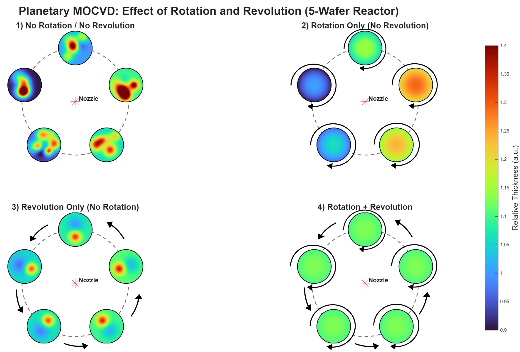
Wafers are called satellites as they have two types of motions: a) its own rotation; b) revolution around the susceptor. The motion is similar to planets around the sun, hence the name. Rotation and revolution makes sure most of the area of the wafer is equally exposed to precursors. Rotation decreases thickness and compositional variations on a wafer and imparts a somewhat predictable radial symmetry to the thickness and compositional profiles.


The reason for such a rotation and revolution scheme is because thickness needs to be uniform for ideal device formation across the wafer. The precursor gases are distributed near equally in all directions but, controlling the concentration of gas inside the chamber is not possible. One area of the susceptor will be exposed to more gas than the other areas. Similarly, the area of the wafer near to the nozzle will receive a higher amount of precursor gas exposure resulting in a taller structure to form.
What happens if we do not rotate the wafers around the susceptor?
Non-uniform distribution of gas around the cahmber will result in high thickness variation in all wafers. Device performance, reproducibility, and repaetability get hurt impacting industrial adoption.

The plot in figure 5 shows the thickness profile expected on the wafer during deposition. Most of the growth will be concentrated near the nizzle due to high concentration of precursor gas. Growth rate rises rapidly as precursors first reach the heated substrate, reaches a maximum somewhat upstream of the wafer center, and then gradually decreases due to precursor depletion and boundary-layer thickening. A skewed Gaussian curve with an exponential depletion tail is how it is portrayed in theory.

Figure 6 details the difference in thickness variation across wafers under different scenarios. Completely stationary wafers will show maximum randomness in thickness measurements due to non-uniform gas flow in chamber and constant nozzle distance of every growth point on the wafer. Rotation will allow uniform growth of layer but across all wafers that uniformity is absent, every wafer has a different thickness due to unequal precursor distribution. Revolution solves the problem of unequal gas distribution by allowing wafers to change locations around the chamber resulting in near uniform thickness across all wafers.
Gas Foil Rotation
Planteray motion in MOCVD reactors is possible through the use of gas foil rotation technology. The wafer rotates on a satellite plate which has gas flowing underneath. The gas pushes the plate up and hovers it. The grooves direct gas flow and the flow rate determines rpm. The gas used is the same as precursor carrier gases, i.e., nitrogen and hydrogen.
The carriers are introduced through openings grooves in the susceptor body. The gas enters the narrow gap between the susceptor and the satellite, where it flows through spiral grooves on the underside of the satellite. The pressure generated within the gas film provides a lifting force that levitates the satellite, while the flowing gas’s interaction with the spiral groove walls generates a tangential force that causes the satellite to rotate.

Temperature Sytems
Heating is achieved by RF inductive heating. An RF coil surrounds the reactor chamber. Alternating current in the coil generates a magnetic field. This induces eddy currents in the graphite susceptor, producing heat.

Proper cooling measures are equally important to protect electronics and the user. Cooling water is used to chill reactor walls and prevent overheating of the reactor housing. It maintains stable thermal conditions inside the chamber. Carrier gases also contribute in removing heat by conduction.
In-situ Monitoring
This term refers to the monitoring of gas and film thickness during the process.
- Reflectometry: Monitors the intensity of light reflected from the wafer surface during growth. It can provide us with growth rate (nm/min or µm/hr, layer thickness, surface quality and smoothness, and the detection of the start and end of layer growth.
- Pyrometry: Measures the wafer surface temperature using infrared radiation emitted by the heated wafer. It provides us with real-time non-contact temperature measurement during growth.
- EpiRAS: Reflectance anisotropy spectroscopy. This technique monitors surface reconstruction and crystal structure changes during growth by measuring anisotropy in reflected polarized light.
- Pressure and Gas Monitoring:
- Pressure gauges for chamber pressure control
- Mass flow controllers (MFCs) for gas flow rates
- Gas concentration sensors to verify precursor delivery.
Reactor Gas Delivery System
The reactor delivery system, or gas panel, is a very clean, leak-free network of stainless-steel tubing, automatic valves, and electronic mass flow controllers. Each constituent or dopant type (e.g., gaseous hydride, high vapor pressure liquid, etc.) requires a different control stream, which is replicated for each source of the same type. Hydride delivery modules generally require a few valves and an electronic mass flow controller, since these sources are already
provided as dilute, high-pressure gases in gas cylinders. Liquid alkyl delivery modules are more complicated. These high-vapor-pressure source materials are contained in stainless-steel bubblers and held in a refrigerated bath to maintain a stable vapor pressure over the liquid or solid source. Additional plumbing is provided for source replacement without contamination of the rest of the delivery system. If a fixed relationship is maintained among the total pressures in all vent and supply lines, transients will be minimized and the actual source flow can be controlled.

Constant source delivery is critical for compound semiconductor devices and can have implications in the growth of thicker heterostructures in materials systems that must be lattice matched. Small changes in carrier gas flow can significantly change the source delivery. Therefore, the design of gas delivery systems must avoid transients from switching or dead space. To improve carrier gas consistency further, the vent-run system maintains a relatively large flow rate of carrier gas (typically several litres/min) in the supply line.
Often there are separate hydride and alkyl supply lines. Special vent-run valves that have nearly zero dead space couple the individual source modules to the supply line. The source flow rate (usually on the order of tens or hundreds of cm /min) can then be established and stabilized while the valve is vented to a waste line
Safety Measures
Hydrides pose the biggest risk because they are high-pressure toxic gases. The alkyls pose the next highest risk because, although they are toxic and pyrophoric, they are liquids and generally easier to handle. Some of the effluent gases cause risk because they can contain elemental phosphorus and arsenic as well as the oxides of these elements. Ancillary risks include quartz reaction chambers (which are breakable), large volumes of explosive hydrogen gas, high temperatures, and the acids and solvents used for preparing for, and cleaning up after, a growth run.
Frequently Asked Questions (FAQ)
Ques: What is epitaxy?
It is the technique used to grow a thin crystalline film (epitaxial layer) on a crystalline substrate, where the deposited layer adopts the crystal structure and orientation of the substrate.
Ques: What is the difference between growth and deposition?
Deposition is the process of adding material onto a substrate from external sources to form a thin film or coating. Examples include PECVD, sputtering, and ALD, where the substrate primarily acts as a surface on which the material is deposited.
Growth refers to the formation of a material layer through chemical reactions and atomic incorporation at the substrate surface, often with the substrate influencing the film’s crystal structure or directly participating in the process. Examples include GaN epitaxial growth by MOCVD and thermal oxide growth on silicon.
In short, deposition emphasizes the addition of externally supplied material, while growth emphasizes the formation and development of the film at the substrate surface.
Ques: What is MOCVD?
It is the process of growing compound semiconductor layers on a wafer using pyrolysis reactions between the vapours of a volatile organometallic compound and a gaseous hydride.
Ques: What is a pyrolysis reaction?
It is the degradation of compounds in the absence of oxygen at high temperatures ranging from 500℃ to 1200℃.
Ques: Who is Aixtron?
AIXTRON is a German technology company that develops and manufactures deposition equipment used in the semiconductor industry. Its systems are widely used for the production of compound semiconductors such as GaN, GaAs, and SiC, which are used in LEDs, power electronics, RF devices, and advanced communication systems. AIXTRON is particularly known for its Metal-Organic Chemical Vapor Deposition (MOCVD) equipment.
Ques: What does in-situ mean?
In-situ is a Latin term meaning “in the original place” or “on site.” In science and engineering, it refers to measurements, observations, or processes carried out directly within the system or environment where they occur, without removing the sample. For example, in semiconductor manufacturing, in-situ monitoring techniques measure growth conditions inside the reactor during deposition, allowing real-time process control.


Leave a Reply